SCREW: SCalable and Reproducible Exfoliation of epitaxial graphene grown on silicon carbide Wafers
SCREW: Exfoliació escalable i reproduïble de grafè epitaxial dipositat sobre oblies de carbur de silici (2019 LLAV 00052)
OT1: Promoure el desenvolupament tecnològic, la innovació i una investigació de qualitat.
Aquest projecte està cofinançat pel Fons Europeus de Desenvolupament Regional (FEDER) de la Unió Europeaen el marc del Programa operatiu FEDER de Catalunya 2014-2020 amb un ajut de 20.000 €
Advanced or emerging materials, such as graphene, require the development of new processing technologies for eventually delivering real applications. A paradigmatic bottleneck in graphene applications for the electrical and electronics engineering industries is the poor quality or limited readiness of some types of synthetic graphene.
Basically two strategies outstand for their crystal high quality and relevance for eventual industrial adoption, chemical vapour deposition graphene (CVD-G) and epitaxial graphene on silicon carbide (EG-SIC). CVD-G cannot be immediately used for devices in its as-grown substrate (typically transition metal foils), thus, CVD-G needs to be transferred to electronics technical substrates, such as silicon oxide. This typically implies, for instance, sacrificial etching of the catalytic metal in aggressive chemical solutions such as iron chloride and is time consuming.
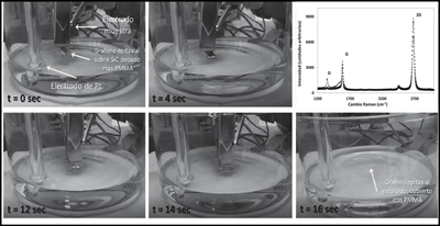
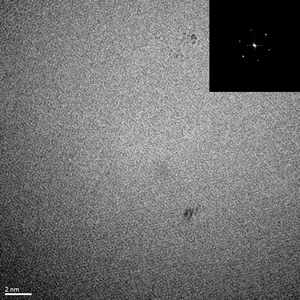
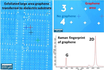
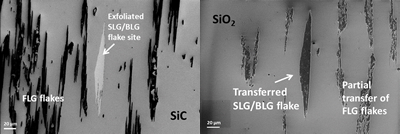
At the IMB-CNM-CSIC, we achieved for the first time to delaminate and transfer EG-SiC by applying an electrochemical method on a safer saline solutions and the hydrogen bubbling mechanism (Figure 1). The SCREW project aims to benchmark the process scalability, improve exfoliated graphene materials yield (Figure 2) and quality (Figure 3), for increasing its TRL and versatility (Figure 4) and assessing the technology transfer potential of our patented method.